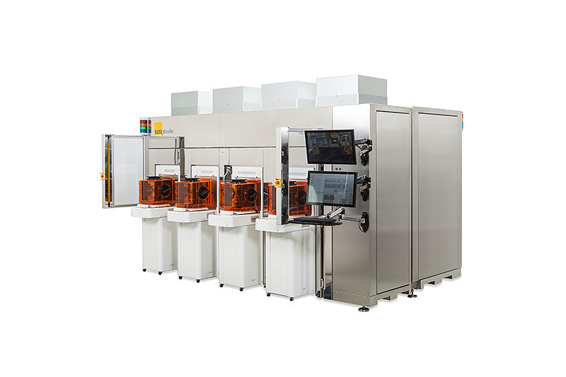
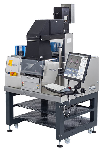
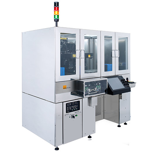
A mask with a certain structure is aligned with the wafer in very close proximity (thus “proximity” lithography). During exposure, the shadow cast by the mask structure is transferred to the wafer. The resulting exposure quality depends on both the precision with which the mask and wafer are spaced apart and the optical system used for exposure.
Being fast and suited to flexible implementation, this method is regarded as the most cost-effective technique for producing microstructures down to 3 µm in size. With contact exposure, resolutions in the sub-micron range can be achieved. Typical areas of use include wafer-level chip-scale packaging, flip chip packaging, bumping, MEMS, LED and power devices. The systems are deployed in high-volume production as well as in industrial research.
The mask aligners supplied by SUSS MicroTec are based on proximity lithography.
Features & Benefits
Superior resolution as a result of diffraction-reducing optics
Process stability through the use of microlens optical systems
Available for:
Automated Mask Aligner
· MA300 Gen2
· MA200 Gen3
· MA100/150e Gen2
Semi-Automated Mask Aligner
· MA12
· MA/BA Gen4 Pro series
· MA/BA Gen4 series
· MA/BA6
Manual Mask Aligner
· MJB4


